Rapidus Corp., the Japanese government-backed foundry consortium betting that Tokyo can re-enter cutting-edge logic manufacturing, ran its first 2nm test wafers through extreme ultraviolet lithography at the IIM-1 plant in Chitose, Hokkaido this month, marking the most consequential milestone yet for a project that has consumed roughly $11 billion in public money and another $25 billion-plus in committed industry capital. The pilot wafer step keeps Rapidus on its publicly committed timeline to begin commercial 2nm production in 2027, even as it leaves the company roughly 18 months behind market leader TSMC, whose Hsinchu Fab 20 has been shipping N2 silicon since late 2025.
The technical bar
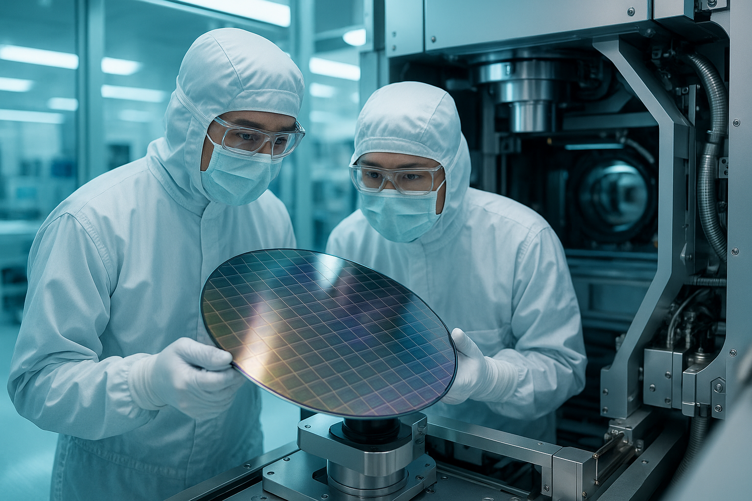
The pilot run uses gate-all-around (GAA) nanosheet transistors, the same architecture deployed by TSMC’s N2 and Samsung’s SF2 nodes, derived from a 2022 technology-licensing agreement with IBM Research’s Albany center. Rapidus CEO Atsuyoshi Koike told reporters at a media briefing in Chitose this month that the IIM-1 line is now running with two ASML NXE:3800E EUV systems and that a third tool is scheduled for installation this summer (Nikkei). The test wafers are not yet at design-for-yield density and are intended to validate the full process module flow; commercial-grade defect targets are expected to be set in the second half of 2026.
The factory’s most distinctive operational bet is its single-wafer processing model, in which every step is run on individual wafers rather than 25-wafer lots. Rapidus argues this lets it ship customer prototypes faster and offer per-wafer pricing rather than per-lot pricing, a positioning aimed squarely at the U.S. AI-chip startups that have been priced out of TSMC’s allocation. Koike confirmed letters of intent with two unnamed North American customers but declined to identify them.
The financial scaffolding
Japan’s Ministry of Economy, Trade and Industry has now committed roughly Y1.72 trillion ($11.2 billion) to Rapidus across three tranches since 2022, the largest single industrial subsidy in modern Japanese history (METI). The consortium itself, comprising Toyota, Sony, NTT, NEC, SoftBank, Denso, Kioxia and Mitsubishi UFJ Bank, has put in around $500 million in equity, with another $25 billion to $30 billion in capital expenditure expected through commercial ramp. The most recent tranche, Y802 billion approved in March, was contingent on this pilot wafer milestone (Reuters).
Critics inside Japan’s industrial policy community argue the program is structurally undercapitalized. TSMC will spend roughly $40 billion on capex in 2026 alone, and Samsung’s foundry division around $24 billion. Rapidus’ total committed lifetime budget is on par with a single year of either rival’s spend.
What it means for the global foundry race
The Rapidus milestone narrows but does not close the cutting-edge logic gap among the four players currently building 2nm-class lines. TSMC remains the volume leader; Samsung’s SF2 yields recently crossed reported thresholds for Qualcomm tape-outs; Intel’s 18A node is in risk production at Fab 52 in Arizona; and Rapidus now has running silicon. For customers, the practical effect is that 2027 will be the first year in two decades with four geographically diversified sources of leading-edge logic, a structural change that Washington, Brussels and Tokyo have all spent the past four years trying to engineer through subsidies. Whether Rapidus can convert pilot wafers into yielding commercial product remains the open question, and the one METI’s next funding decision will turn on.


Discussion
Sign in to join the discussion.
No comments yet. Be the first to share your thoughts.